 ESPCI web site


S. Holé, J. Lucas, Y. Oussar, C. Filloy
Under high voltage, charges can be injected from electrodes and accumulate inside an insulator. Some parts of the insulator are then submitted to an electric field higher than the nominal electric field, a situation that can lead to breakdown and even to failures in the system in which the insulator is included. Understanding charge phenomena requires sophisticated non-destructive measurement systems and precise signal analyzes. We are particularly involved in this two points by proposing precise measurement models for the three main direct measurement methods and simple ways to analyze the different contributions to the signal in order to avoid any misinterpretations, specially in non-uniform materials. In that latter case we had shown that the signal produced by any of the three main direct measurement methods is drastically impacted by non-uniformity in the tested material. As an illustration a typical signal with a laminate material under voltage is shown in Figure 1a in which spurious oscillations are mixed with charge signal. The main difficulty with non-uniform materials is the assumption of their internal structure which may induces errors in the charge estimation. Nevertheless we have shown that a judicious calibration measurement can be used as an assumption of the internal structure of the nonuniform material. The estimation of the charge distribution is then much less erratic and the signal can be treated as if it were obtained with a uniform material. The treated signal in Figure 1b shows indeed a rapid charge buildup at the anode and a slower at the anode.
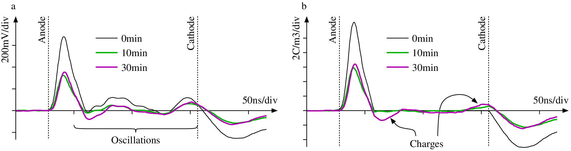
- Fig 1: (a) Typical signal in a non-uniform material. Oscillations are not due to charges but to non uniformity. (b) Charge distribution estimation in a non-uniform material after corrections.
The measurement of charge distribution has attracted numerous industrial collaborations (SAGEM, GE Healthcare, Nexans) for studying specific materials as well as academic collaborations (LAPLACE, IES) to work on measurement techniques in order to improve spatial resolution by a factor 10 at least and to reach the nanometer scale.
The numerous modelings of the space charge distribution measurement methods have shed new light on various sensor physics, specially for capacitive sensors. We have then derived analytic tools for estimating the sensitivity map of capacitive sensors and used them in the context of industrial collaborations (Hitachi, Bostik) and within the framework of the OMICAGE ANR program for estimating the water content in wood-chips, a promising sustainable energy fuel.
In the case of electrostatic sensors is the development of efficient ionic smoke sensors. It has to be said that too kinds of smoke sensor exists, optical smoke sensors and ionic smoke sensors. Conventional ionic smoke sensors are far more efficient, in terms of sensitivity and response time, than optical smoke sensors. However they usually use a minute quantity of americium 241, a radioelement that releases alpha particles to ionize surrounding air. That radioelement is no longer desirable, mainly because of recycling problems, then ionic smoke sensors are progressively forbidden in any countries. In order to continue to benefit of the efficiency of these kinds of sensors we have proposed a kind of ionic smoke sensors based on a corona discharge. Figure 2 shows the response to smoke of these two kinds of ionic smoke sensor which can respond more than one minute prior to optic sensors.
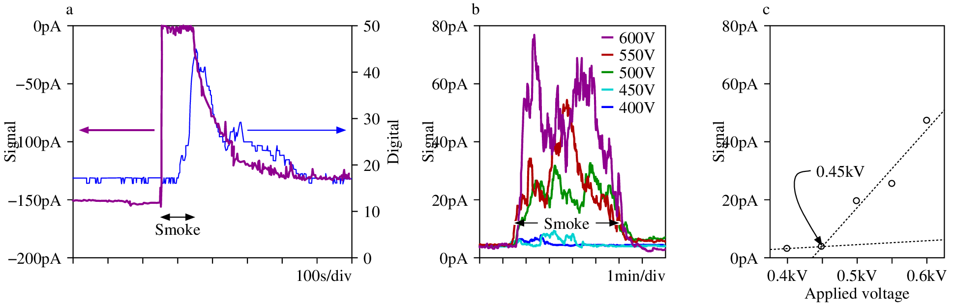
- Fig 2: (a) Smoke detection by the reduction of the current in a drift chamber as soon as smoke enter the sensor. Comparison with an industrial optic sensor which responds more than one minute after our ionic smoke sensor. (b) Smoke detection by a corona discharge triggering. A discharge is triggered as soon as smoke enter the sensor. (c) The detection threshold is 450 V.